 Up until now the Intel system
architecture has traditionally consisted of a three chip solution;
processor, memory controller hub (MCH) also known as the Northbridge chipset,
and I/O controller hub (ICH) commonly called the Southbridge chipset. This
CPU-Northbridge-Southbridge arrangement happily survived many years of
upgrading intact. Yet as memory speeds increased, CPUs gained extra
processing cores and videocards grew more powerful, the interconnects that
allowed all these components to communicate increasingly became swamped
with data. The solution Intel implemented was to move the memory controller
from a discreet chipset directly onto the processor itself - a technique that
AMD had opted for several years prior with its Athlon 64 processors.
An integrated memory controller was introduced for the Intel
platform with the high end Core i7 'Nehalem' processor about a year
ago. By moving the memory controller onto the CPU, Intel simplified its platform
to the processor-southbridge architecture we see today.
The Intel Core i5 'Lynnfield' P55 platform follows in these footsteps.
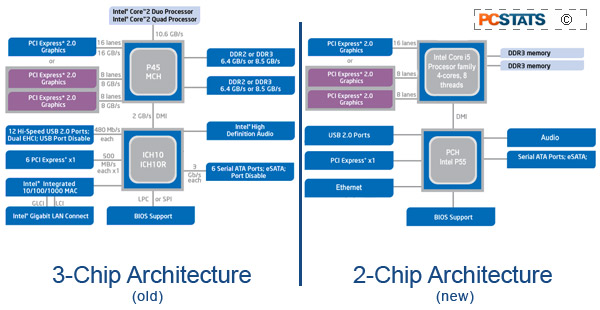
Here's a block diagram to illustrate the differences between legacy Intel
platforms (left) and the current "Lynnfield" platform (right) that
underpins the Core i5 processor and Intel P55 Express chipset. The main
difference is that tasks previously handed by the Northbridge chipset are now
rolled into the Core i5 processor proper.
Intel's P55 Express chipset integrates both the memory controller
and sixteen PCI Express 2.0 lanes on to the die of the "Lynnfield"
CPU. The P55 Express Platform Controller Hub has eight further PCI Express
lanes at its disposal. This shift in the PCI Express graphics sub-system doesn't
have a huge impact on end-users, most P55-based motherboards still have two
or three PCI Express x6 videocard slots that can be run in (x16/x4) or
(x8/x8/x4) mode, the only change is that now the first two slots are handled
directly by the CPU.
|
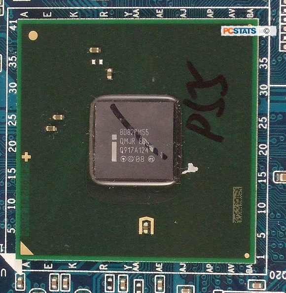
Intel P55 Express. It replaces the P45 Express and Intel ICH10
pairing.
|
For gamers, both NVIDIA SLI and ATI CrossfireX multi-videocard
technologies are supported by Intel P55 Express chipset, though
implementation varies with each motherboard. Socket-1156
"Lynnfield"-compatible motherboards are DDR3-exclusive, and support memory
speeds from DDR3-800 up to DDR3-1333, with overclocking going all the way up to
DDR3-2000+ in some cases.
Since Intel's P55 Express doesn't have too many roles left to do (since
graphics and memory communication are now handled by the CPU), it actually
doesn't need a very fast link to the processor. Instead of equipping the Intel
P55 express chipset with a complex and expensive-to-produce QPI link, Intel has
instead selected a slower 2.0GB/s DMI link for the Intel P55 Platform Controller
Hub to communicate with the processor. Both northbridge and southbridge have
been merged into what Intel is now calling the P55 Platform Controller Hub.
Storage and media interface capabilities are pretty similar to that of
Intel's well-known ICH10R southbridge, which include support for fourteen USB
2.0 ports, six SATA 3Gb/s ports with support for RAID 0/1/5/10 and Gigabit
Ethernet.
Intel's LGA 1156 CPU Socket
Intel Core i5 and Core i7 800-series processors use a new LGA
1156 socket that is not backwards compatible with socket LGA775 Core 2
processors. Let's take a quick look at the socket 1156 on the GA-P55-UD5
motherboard.
|
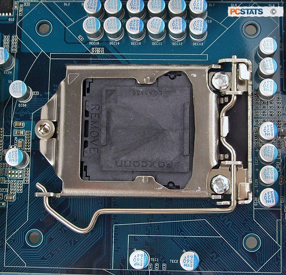
This is the Core i5 socket 1156 - notice
anything different?
|
The LGA1156 socket is a physically different shape than previous 775/1366 processor sockets so
there won't be an issues with mistakenly installing an older chip into it. It's
not compatible with any socket 775 heatsink either. The four
holes around the CPU socket are spaced a little bit differently so they will NOT
line up with socket 775 mounting brackets. Heatsink and fan manufacturers
rejoice, people will need to buy entirely new coolers because of this.
|
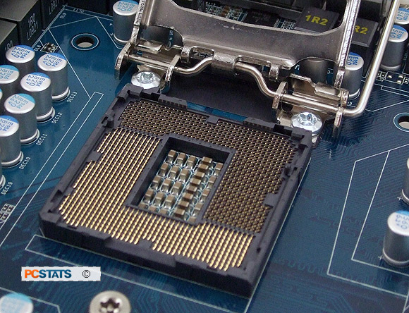
Like LGA775 processors, the LGA1156 Core i5 chips
are pinless.
|
For whatever reasons, Intel LGA775, LGA1156 and LGA1366 heatsink mounting
hole spacings are all a bit different (72mm, 75mm and 80mm on center
respectively). The same injection molded plastic Intel C33389 reference fastener
is used on all three thermal solution systems, so we don't understand why Intel
didn't just pick a standard new size, say 80mm, and stick to that for Core i5
and Core i3 processors.
Now let's take a walk around the rest of the Gigabyte GA-P55-UD5 motherboard.
