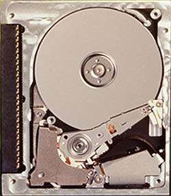
IBM 1GB Microdrive
--IBM
is tripling the capacity -- but not the size -- of theworld's smallest hard disk
drive, paving the way for a new generation of "go-anywhere" pervasive-computing
devices and applications.
 Packing one gigabyte (GB) of data storage capacity on to a disk the size of an American quarter, IBM's newest Microdrive can hold up to 1,000 high-resolution photographs, a thousand 200-page novels or nearly 18 hours of high-quality digital audio music.
The 1 GB Microdrive brings affordable high-capacity, high-performance data storage to a wide variety of handheld electronic products -- including digital cameras, handheld PCs, personal digital assistants (PDAs), portable Internet music players and video cameras. It can also serve as a data-exchange accessory to notebook computers, desktop computers and printers. Future applications may include wearable computers, electronic books, global positioning system (GPS) receivers, smart phones and electronic wallets.
"Using the new Microdrive, a company's entire multimedia product catalog -- as well as a suite of powerful e-business applications -- can be carried around in a shirt pocket," said Michael Kuptz, director, IBM Microdrive Products. "Such vast capacity in such a compact size will dramatically change the way information technology and consumer electronics devices are designed and used, helping accelerate the worldwide adoption of pervasive computing."
Underscoring the dramatic pace of development in the storage industry, IBM introduced the world's first gigabyte-capacity disk drive, the 3380, in 1980. It was the size of a refrigerator, weighed 550 pounds (about 250 kg) and cost $40,000. The Microdrive announced today is smaller than a matchbook, weighs less than an ounce and will be available for less than $500.
Limited quantities of the 1 GB Microdrive will begin shipping in July to original equipment manufacturers (OEMs) and distributors. Retail shipment is scheduled for September. Customers that have designed or plan to design devices compatible with the new Microdrive include Acer, Casio Computer Co., Ltd., the IBM Personal Systems Group, Eastman Kodak Company, Fuji Photo Film Co., Ltd., Hewlett-Packard, i2Go, Minolta Co., Ltd., Nikon Corporation, Psion, RICOH Co., Ltd., and Sanyo Electric Co., Ltd.
IBM CMOS 9S Chip Technology
 --IBM today announced it has launched production of powerful new microchips for servers, communications gear and pervasive computing products, using the most advanced chip-making technology ever developed.
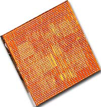
The new technology, named CMOS 9S, unites -- for the first time -- IBM innovations in copper wiring, silicon-on-insulator (SOI) transistors and improved, "low-k dielectric" insulation to build chip circuits as small as 0.13 microns, or nearly 800 times thinner than a human hair. The smaller circuitry and improved materials can pack more processing power on a single chip, helping electronic products from computers to cell phones support new, performance-hungry applications like speech recognition, fingerprint authentication and wireless video.
A variety of chips are already in pilot production using IBM's new manufacturing technique, with first customer shipments planned for early 2001.
"Our new chip-making recipe integrates more complex, high-performance ingredients onto a chip than ever before," said Bijan Davari, IBM Fellow and vice president of technology and emerging products for IBM. "This unique technology can help meet exploding customer demand for higher performance, higher function products. The integration of SOI, copper and low-k insulation offers a powerful combination of technologies which maintains our two to three-year technological lead."
CMOS 9S is optimized to manufacture complex chips containing hundreds of millions of high-speed transistors and miles of microscopic copper wiring. The technology features the smallest SRAM memory cell in production at 2.16 square microns, which allows for more high-performance memory to be placed directly onto a chip, resulting in faster, more efficient processors.
CMOS 9S is the only 0.13-micron technology to take advantage of the performance benefits of SOI, which dramatically improves transistor performance -- up to 35% -- by providing an insulating layer in the silicon base of a chip, thereby isolating the transistor and improving the flow of electrical current to the chip's circuitry.
When combined with up to nine layers of copper wiring, available only in IBM's CMOS 9S, SOI can be used to meet higher performance and/or lower power requirements required by 0.13-micron chip designs. By boosting chip performance and reducing chip power requirements, SOI is critical for chips that will power a wide range of products, such as Internet servers or wireless communications gear.
CMOS 9S also uses another IBM chip-making breakthrough -- "low-k dielectric" insulation -- to meticulously shield millions of individual copper circuits on a chip, reducing electrical interference between wires that can hinder chip performance and waste power. IBM was the first semiconductor manufacturer to perfect a technique for building chips with a true low-k dielectric material which better insulates copper wiring, helping electronic signals move faster and more efficiently through a chip.
IBM is producing chips using the new CMOS 9S process on a pilot production line in its Semiconductor Research and Development Center in East Fishkill, NY and intends to introduce the technology on its high-volume Burlington, VT, manufacturing lines early in 2001. This new manufacturing technique will be used to produce future generations of the IBM POWER4 processor, which will ship in a next-generation IBM eServer(a), code named "Regatta," next year.
