NVIDIA
While bits and pieces of information have slowly surfaced regarding NVIDIA's
nForce chipset, the official hardware disclosure took place at the lavish
Formosa Hotel some 30 minutes away from the show floor. Proffering support for
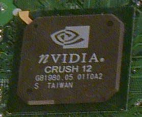
AMD's Athlon and Duron processors, the NV22 (otherwise known as the Crush 11/12)
is arguably one of the most exciting chipset designs in that it leverages the
latest bus technologies as well as the first graphics core with truly acceptable
3D performance. Like most competing products, the nForce is split between a
North Bridge (Integrated Graphics Processor) and a South Bridge (Media and
Communications Processor).

Serving as a means of communication between the processor, memory, and
external AGP controller, the ICP's primary feature is an integrated GeForce2 MX
graphics core, meaning it has two pixel pipelines clocked at 175MHz. Since the
logic is intertwined with the rest of the core logic, NVIDIA has been able to
utilize an equivalent AGP 6x interface, bolstering AGP throughput. In its
current form, the extra AGP bandwidth will probably not be utilized, since the
bus has yet to be saturated with geometric traffic and AGP texturing is still
very detrimental to performance.
Currently, the most common factor limiting the performance of 3D graphics
is memory bandwidth. Of course, each manufacturer recognizes this and is
attacking the problem in a different way. In building the GeForce3, NVIDIA implemented
a crossbar memory controller that was made up of four 32-bit DDR
controllers rather than a single 128-bit unit. With this scheme, memory could be
accessed more efficiently and in smaller blocks, reducing wasted data transfers.
A similar idea has been put into effect for the nForce chipset, using
dual, independent, 64-bit DDR memory busses. The result is a breathtaking 4.2GB/s
of memory bandwidth shared between the host processor and the integrated graphics -
each of which can access either of the memory controllers. However, in order to
take advantage of both memory controllers, two DIMM modules need to be
installed.
NVIDIA's second new technology is called the Dynamic Adaptive Speculative
Pre-Processor and involves pre-fetching data that the chipset believes the
processor will request before the request is made. If the prediction is correct,
then the data is sent directly from the on-chip cache rather than retrieved from
main memory. Conversely, if the data is not needed, the only loss is memory
bandwidth that would not have otherwise been utilized.
In the interest of staying competitive with other chipset makers, NVIDIA has incorporated
a host of standard features into their MCP, such as dual ATA-100 controllers,
a software modem, 10/100 Ethernet, six USB ports, and an AC 97
codec. The Audio Processing Unit integrated into the MCP is fully DirectX 8.0
compliant and according to NVIDIA, is the same technology used to power
Microsoft's XBox. In its most feature-complete form, the MCP also includes a
Dolby Digital encoder, capable of passing Dolby Digital content to an external
decoder where the signal can be sent to each of up to six speakers.
 The final key in linking the components of nForce together is AMD's
HyperTransport I/O bus. Like VIA's V-Link, NVIDA has opted for an 8-bit
implementation, however, by running the bus at 200MHz DDR, throughput shoots up
to 800MB/s. If more bandwidth is needed at a later date the bus can be expanded,
but for the time being it should provide ample room to eliminate any I/O
bottlenecks that may have previously existed.
Ultimately, the deciding factor in the success of NVIDIA's nForce will be the
target audience. Performance enthusiasts eyeing the chipset could care less about
GeForce2 MX-style graphics, meaning they will be paying a premium for a feature
that will never be used, while those who concern themselves with value will not
want to pay the price of admission. If overall performance of the chipset does
not justify the added cost, nForce will be a tough sell in the midst of SiS and
VIA vying for high-end dominance in the Socket 462 market.
