|
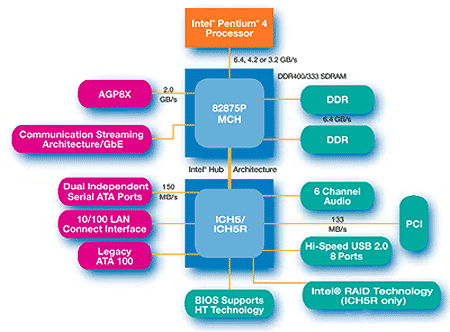
Cast aside the i850E chipset and RDRAM which have gone the way of the dodo, and the new king of the hill is clearly Intel's i875P chipset a.k.a. "Canterwood."
89% Rating: 
|
|
|
|
Home >
Reviews >
Motherboards >
AOpen AX4C Max |
|
|
Enter the i875P Canterwood
While many of the specifications of the i865PE Springdale
and i875P Canterwood chipsets appear to be quite similar, the i875P does
in fact use a bigger BGA and actually has more solder balls on the bottom of
the packaging. In other words they are quite different chipsets.

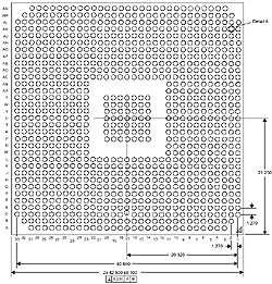
The FCBGA i875P measures 42.5 x
42.5mm and uses a total of 1005 balls to connect to the motherboard. The i865PE is
physically a bit smaller at 37.5 x 37.5 mm, and is connected to the motherboard by
just 760 balls. On an interesting note, the i875P outputs approximately 12.1W of
heat when running all four DDR DIMM's in dual channel 400 MHz mode with an 800 MHz
FSB chip.
The i865PE chipset outputs a maximum of 11.3W
of heat energy while running four DIMM's in Dual channel 400MHz memory mode under 800 MHz FSB; so
it basically runs a bit cooler, but not by much. Both the i875P and i865PE chipsets can run up to a maximum temperature of 99 degrees Celsius, or until
the solder balls start melting. ;-)
 
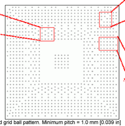
Base of the i875P chipset shown at Left, i865PE at Right.
There are two obvious features that the i875P chipset has
that the i865PE chipset does not. The first is ECC memory support and
the second is a technology known as "PAT". No, PAT is not a
androgynous character from Saturday Night Live
, though
you would have thought Intel could have chosen something a bit more catchy to describe what they
term "Performance Accelerating Technology."
Support for ECC DDR memory
is not too surprising since Intel are targeting workstation users
as well mainstream desktops with the i875P chipset. Data integrity is more important than
anything else in the workstation world after all. In the desktop world though, ECC
has not really caught on with the average user due to the higher costs and
minimal data integrity advantages.

For a company that came up with NetBurst, Hub Architecture
and SSE2, Performance Acceleration Technology
seems like a very tame
advancement. PAT basically works inside the memory controller to run things a bit more
efficiently. As the example above shows (from Canterwood PowerPoint
presentation), between the processor and memory controller PAT saves the system 1
clock cycle and from the memory controller to system memory
we save another clock cycle.
While saving two memory clock cycles may not sound like a
lot, when you consider the billions of calculations that are relayed between the
processor, memory controller and system RAM, it can a huge
difference if you believe what Intel says. What is
really interesting with Canterwood is something called Communications Streaming Architecture, which we'll deal
with next...
|
