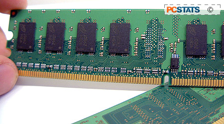
The DDR2 standard also includes some improvements
over DDR which help make the new memory more efficient, both at transferring
data and at saving power:
On Die Termination (ODT) is built into
each DDR2 memory chip on a module. Instead of having terminating resistors built
into the motherboard to eliminate excess electrical 'noise' in the signal of the memory bus,
DDR2 builds a resistor into each chip, deactivating it when the
chip is in use and reactivating it when the chip is in standby.
This apparently decreases signal interference while transferring data to and from the memory by
moving the termination closer to the source, preventing interference within the module itself. This isn't
something the end user has to worry about, but for electrical engineers,
ensuring signal interference is lessened, allows the memory to function more
reliably.
Posted CAS and additive latency are two new
technologies which work hand in hand to eliminate data collisions within memory.
In conventional DDR memory it is possible for a bank activation and a read
command to occur on the same clock cycle, causing a collision and forcing the
activation command to be shifted by one clock cycle.  This results in a read command from the shifted activation
command being shifted one clock cycle, and so on. This creates a gap in
memory transfers when it happens, reducing bandwidth.
With posted CAS and additive latency, a read
command is issued immediately after the activate command, then this read command
is delayed internally by a predetermined amount of clock cycles (hence additive
latency) before being executed. As this action is done without need for an
additional command, no collision will occur. This holds true even if
another activate command is issued on the same clock cycle the read command
eventually executes on.
What about Latency issues?
Latency is one area where the DDR2 specs fall short of regular
DDR memory, at least on paper. The JEDEC definition of DDR2 allows for
CAS latencies of 3,4 or 5, as compared to DDR's 1.5,2 and 2.5. While some
manufacturers have released 400MHz DDR2 at CAS latency 3, all 533MHz DDR2 chips
currently shipping use a Latency timing of 4-4-4. As 533MHz DDR2 is likely
to be the first widely used speed for the new standard, these are the timings
that will be the default standard.
Write latency is also considerably greater with
DDR2. While DDR1 allows a single cycle for write latency (1T), DDR2
defines write latency as read latency-1. This means that with a CAS
latency of 4, DDR2-533 should have an effective write latency of 3T. Again
this seems like bad news on paper.
To be
fair, it may be difficult to compare DDR2 to DDR memory directly in terms of
latency and performance. The various new features that DDR2 implements may make
the difference in memory latency less significant. For more information, check
out PCstats' great article on the benefits of low
memory latency versus memory speed with
respect to DDR, and for a (much) more technical examination of the latency
issues of DDR2 memory, look here.
As it stands, it seems unlikely that DDR2 memory
will have any performance advantage over DDR of an equivalent speed. The
slower speed of the DDR2 core is cancelled out by its ability to move more data
each clock cycle. Manufacturers claim that the various new signal
enhancement features that DDR2 possesses will add to effective bandwidth by
reducing interference, but then DDR2 takes more time to perform data actions
(higher latency). Only proper lab tests will decide this. Stay tuned.
