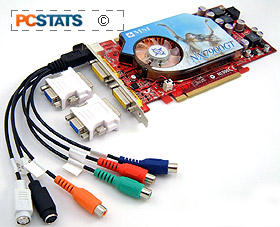
The GeForce 7900GT name should indicate to users that the difference between it
and the preceding GeForce 7800GT/GTX is minimal (unlike the jump from GeForce 6800
to GeForce 7800).
 Aside from the improved manufacturing process which results in a smaller core size,
and lower cost, there are really no architectural differences between the
'G70' and 'G71' GPUs.
If you recall, nVIDIA chose to stick with 0.11 micron manufacturing
process for the 'G70' and instead experimented with newer manufacturing
techniques on its lower end products. Now that TSMC has the 0.09 micron
manufacturing process down pat, nVIDIA has given its 'G70' core a refresh and so
the 'G71' is born.
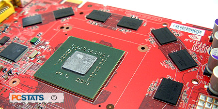
The new nVIDIA GeForce 7900GT core contains a hefty 278 million
transistors (which take up an area of 196 square millimeters vs. 352 square
millimeters for the ATi X1900 core), which is less than the 7800GTX's 302 million. The 7900GT GPU is normally
clocked at 450 MHz but the MSI NX7900GT-VT2D256E-HD GPU is clocked at 500 MHz. Its pixel pipeline has
remained the same at 24, and the vertex pipeline at 8.
 The GeForce 7900GT core continues on with Intellisample 4.0
technology, CineFX 4.0 engine and supports DirectX 9.0C and OpenGL 2.0.
The memory controller remains at 256-bits, and the GDDR3
memory has a default clock speed of 1.3 GHz. Once again the MSI NX7900GT-VT2D256E-HD has its memory clocked higer,
up 210MHz to 1530 MHz. The dual 400 MHz RAMDACs will support dual
monitors with a maximum resolution of 2048x1536 at a staggering 85 Hz. Anyone
with a large 16:9 widescreen LCD will like the fact that GeForce 7900GT series
supports two Dual-link DVI connectors with a maximum resolution up to 2560x1600.
Dual-Link DVI doubles the power of transmissions and provides an increase
in speed and signal quality. This is necessary for extremely high resolutions as
single-link DVI connectors do not support enough bandwidth. For instance, a
single-link DVI at 60 Hz can only display a resolution of 1920x1080, while a DVI
dual-link display can go as high as 2560x1600.
Two new GPUs in the Geforce 7900 Series
Here is a break down of the two new GPUs introduced by nVIDIA as compared
to the current Geforce 7800s. You can see there are a few minor changes between
the classes, but essentially the features are the same.
| GeForce 7900GT/GTX VS 7800GTX
Specifications |
|
7900GTX |
7900GT |
7800GTX-512 |
7800GTX |
| Manufacturing Process |
90nm |
90nm |
110nm |
110nm |
| Number of Transistors |
278M |
278M |
302M |
302M |
| Core Clocks (Vertex, Core in MHz) |
700/650 |
470/450 |
550/550 |
470/430 |
| Memory Clock (MHz / data rate) |
800/1600 |
660/1320 |
850/1700 |
600/1200 |
| Vertex Shaders (#) |
8 |
8 |
8 |
8 |
| Pixel Shaders (#) |
24 |
24 |
24 |
24 |
| Memory Interface |
256-bit |
256-bit |
256-bit |
256-bit |
| Frame Buffer Size |
512MB |
256MB |
512MB |
256MB |
| Memory Bandwidth (GB/s) |
51.2 |
42.2 |
54.4 |
38.4 |
| Verticies/Seconds (million) |
1400 |
940 |
1100 |
940 |
| Texture Fill Rate (# Pixels pipes x clk) in
Billions/sec |
15.6 |
10.8 |
13.2 |
10.32 |
| Bus Technology |
PCI Express |
PCI Express |
PCI Express |
PCI
Express | |
Despite the
die shrink, the power requirements for the GeForce 7900GT have increased from
what the Geforce 7800GT consumes. In a single
7900GT videocard situation, nVIDIA recommends at least a 400W power supply with
22 Amps on the 12V rail. Two GeForce 7900GT videocards running in SLI will
obviously draw more power, and for this nVIDIA recommends power supplies in the
range of 500-600W with 30 Amps on the 12V rail.
In any case, users contemplating a spiffy new GeForce 7900GT videocard
should check out nVIDIA's list of approved
power supplies first.
