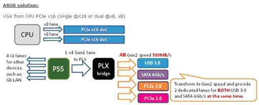
The extra front-end bandwidth the PLX bridge chip provides is a slightly more
elegant solution than plugging the USB 3.0 or SATA 6Gb/s controllers directly
into the P55 PCH's existing PCI Express x1 lanes (which can't handle that amount
of bandwidth individually), and avoids the graphics performance penalty of using
the x16 lanes of PCI Express 2.0 bandwidth provided by Intel's
"Lynnfield/Clarkdale" processors' on board graphics controllers.
|

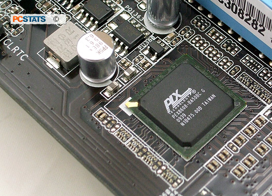
The PLX
PEX8608 chip is a PCI Express 2.0 controller that bridges eight lanes of
PCI Express 2.0 bandwidth between the USB 3.0 and SATA 6Gb/s controllers
to the Intel P55 PCH.
|
However the PLX PEX8608 is still only a bridge
chip, meaning it takes existing bandwidth from the Intel P55 PCH and makes it available at the front-end for the new USB 3.0 and
SATA 6Gb/s storage controllers. The trade off is losing a few expansion slots
that could have taken advantage of the extra PCI Express bandwidth. Before we move
on to the main benchmark section, let's get a little more familiar with Intel's P55
Express chipset.

Intel P55 Express Architecture
 Intel system architecture has traditionally
consisted of a three chip solution; the processor, a memory controller hub (MCH)
and I/O controller hub (ICH). This CPU-Northbridge-Southbridge
arrangement has happily survived many years of upgrading intact.
As memory speeds increased, CPUs gained extra processing cores and videocards
grew more powerful, the interconnects that allowed all these components to
communicate increasingly became swamped with data. The solution Intel
implemented with the Core i7 platform and now with the Core i5 and Core i3
processors was to move the memory controller from a discreet chipset directly
onto the CPU - a technique that AMD pioneered several years prior in the Athlon 64 CPU. By moving the memory controller onto the CPU
itself, Intel simplified its platform to the two chip
processor southbridge architecture of today.
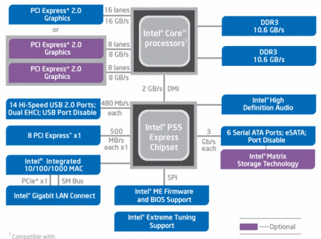
Intel's P55 Express chipset integrates both the memory controller and sixteen
PCI Express 2.0 lanes on to the die of the "Lynnfield" CPU. The P55 Express
Platform Controller Hub has eight further PCI Express lanes at its disposal.
This shift in the PCI Express graphics subsystem doesn't have a huge impact on
end users, most P55-based motherboards still have two or three PCI Express x16
videocard slots that can be run in (x16/x4) or (x8/x8/x4) mode, the only change
is that now the first two slots are handled directly by the CPU.

For gamers, both NVIDIA SLI and ATI CrossfireX multi videocard technologies
are supported by Intel P55 Express chipset, though implementation varies with
each motherboard. Socket 1156 "Lynnfield"-compatible motherboards are
DDR3 exclusive, and support memory speeds from DDR3-800 up to DDR3-1333, with
overclocking going all the way up to DDR3-2000+ in some cases.
Since Intel's P55 Express doesn't have too many roles
left to do (since graphics and memory communication are now handled by the CPU),
it actually doesn't need a very fast link to the processor. Instead of equipping
the Intel P55 express chipset with a complex and expensive to produce QPI link,
Intel has instead selected a slower 2.0GB/s DMI link for the Intel P55 Platform
Controller Hub to communicate with the processor. Both northbridge and
southbridge have been merged into what Intel is now calling the P55 Platform
Controller Hub.
Now that we've covered some of the internals, let's take a quick walk around
the ASUS P7P55D-E Pro motherboard.
