Up until recently desktop computer motherboards have
been built around a three chip solution that hasn't really changed in the past
decade. It consisted of a CPU that communicated directly with the Memory
Controller Hub (MCH) also known as the 'Northbridge,' and this in turn talks to
an I/O Controller Hub (ICH), commonly called the 'Southbridge.'
The CPU-Northbridge-Southbridge architecture happily
survived many years of upgrading intact, but as memory started using more
channels, CPUs grew extra cores and videocards grew more powerful, the
interconnects that let these parts send information to one another became
increasingly swamped with information and prone to bottlenecks. It was time to
redesign the system architecture.
What was once a three chip system has been simplified to
just two parts with Intel's 'Lynnfield' P55 platform: CPU-Southbridge.

In the past couple years Northbridge chipsets for the
Intel platform have included the 945P, 965P, 975X, P35, P45 and so on. Common to
each generation was a discrete silicon chip, and of course, each time some
aspect of the technology advanced an new generation of chipset and motherboard
emerged. This is partly because it's good business to make existing technologies
obsolete, and because a Northbridge chipset acts as bridge between the CPU,
system memory, graphics card and the rest of the PC. Without it the PC cannot
function, and because of their heavy reliance on integration, core logic
chipsets cannot be upgraded like processors.
The third member of the family (the first being the CPU)
is called the Southbridge. It's job is to bridge the CPU-Northbridge with the
rest of the computer; input/output devices like the hard drive, PCI/PCI Express
expansion slots, sound card, network controller and even mouse/keyboard. On the
Intel platform these have included the ICH7, ICH8, ICH9 and ICH10 Southbridge
chipsets.
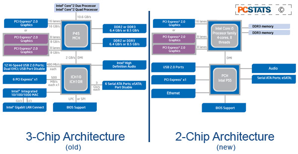
Here's a block diagram to illustrate the relationship
between these three critical chips in a simplified computer system, the way it
has been and the way it has become with the Intel P55 platform. The main
difference between the two is that tasks previously handed by the Northbridge
chipset have been rolled into the Core i5 processor.

So once again, everything you knew about computers has
been stood on its head.
The P55 Express chipset integrates both the memory
controller and 16 PCI Express 2.0 on to the die of the "Lynnfield" CPU. The P55
Express Platform Controller Hub also has up to eight of its own PCI Express
lanes. The changes to the PCI Express graphics sub-system don't have a huge
impact on end-users, most P55 motherboards still have two or three PCI Express
slots that can be run in (x16/x4) or (x8/x8/x4) mode, the only difference is
that now the first two slots are handled directly by the CPU, which has the nice
side effect of removing some system latency.
And there's even better news: both NVIDIA and ATI have
brought SLI and CrossfireX to the Intel P55 Express chipset, so you can use
multiple videocard configurations on certified motherboards.
Although the P55 Express chipset no longer handles
memory itself, its still important to note that memory compatibility on
socket-1156 "Lynnfield"-compatible motherboards is DDR3-exclusive, and runs in
dual-channel mode. Supported memory speeds can run from DDR3-800 up to
DDR3-1333, with overclocking support going all the way up to DDR3-2000+.
Since the P55 Express Northbridge doesn't have many jobs
left to do (with graphics and memory now handled by the CPU), it actually
doesn't need a very fast link to the processor. Instead of equipping the P55
chipset with a complex and expensive-to-produce QPI link, Intel has instead used
a slower 2.0GB/s DMI link for the Intel P55 Platform Controller Hub to
communicate with the processor. Both northbridge and southbridge have been
merged into what Intel calls the Platform Controller Hub.
 The storage and media
interface capabilities are pretty similar to that of Intel's well-known ICH10R
southbridge, with support for 14 USB 2.0 ports, six SATA 3Gb/s ports with
support for RAID 0/1/5 and 10 modes, and gigabit Ethernet.
The Gigabyte Smart 6
Gigabyte
has integrated a suite of software and hardware technologies called the Smart6.
For quite
some time, Gigabyte has placed two Basic Input Output System (BIOS) chips on its
motherboards. The secondary BIOS chip works as a physical backup should the
primary BIOS chip fail. With Smart DualBIOS, Gigabyte has doubled the memory
size from 8MB up to 16MB, and the extra memory means that these BIOS chips can
now do some new tricks. Smart DualBios can save critical data such as passwords
into memory, or even work as a scheduler for important dates and events.
Smart
QuickBoost is a built-in system tuning feature can adjust CPU speed on the fly,
for dynamic processor overclocking inside of windows.
Smart QuickBoost has three levels of overclocking
that will adjust processor speeds up to 400MHz (3x133MHz) above the CPU?s stock
speed. This feature works well when paired with Smart QuickBoot, which has two
modes. The first bypasses BIOS hardware checks that can take a few seconds
during start-up, while the second enables a hybrid S3 (suspend) and S4
(hibernate) state, which allows the system to store its last used state, which
allows the system to power on and resume exactly where it left off last time.
Gigabyte's Smart Recovery utility allows for system backup
by creating snapshots of the hard drive periodically, so it?s possible to
restore deleted or altered files and settings from several different dates in
the past. Smart Recorder is a system logging tool will monitor when your
computer has been turned on or off, as well as keeping a log of when large
amounts of data are transferred between hard drives. Finally, Scheduling using
Gigabyte's Smart Timelock feature can lock down the system during set hours on
certain days of the week, for both system security purposes and parental
control.
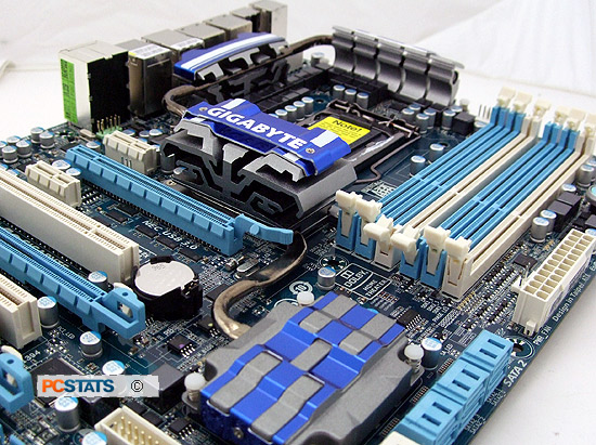
Now let's
take a closer look at the layout of the Gigabyte GA-P55A-UD6
motherboard...
