IBM's CELL Processor: Preview to Greatness?
IBM, in cooperation with fellow industry giants Sony and Toshiba, recently
announced a new processor, called the Cell. While this in itself is not
really cause for much celebration (except perhaps for the odd bedfellows
involved in the project) the new multi-core chip might well prove to be
something special. For one thing, it's going to be at the heart of Sony's
upcoming Playstation 3 console, which we have a feeling may be slightly
popular…
The Cell processor is vastly different from conventional processors inside.
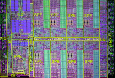
This tiny chip contains a powerful 64-bit Dual-threaded IBM PowerPC core but
also eight proprietary 'Synergistic Processing Elements' (SPEs), essentially
eight more highly specialized mini-computers on the same die.
It's these SPEs that make the Cell architecture special, as
you might guess. IBM describes the product as a 'System on a Chip.' Like IBM's
Power5 processors, multi-processing is build right into the die.
 PCstats is going to take a quick look at what's currently known about the
architecture of the Cell processor and its potential as a rival to today's
x86-based 32 and 64-bit processors.
The basics: Cell Biology
As we mentioned, the prototype Cell processor is composed of a
single 64-bit RISC PowerPC processor and eight SPE 32-bit units. These are
bound together by a fast internal bus, the Elemental Interface Bus (EIB).
A built-in dual channel memory controller is included, and connects to a current
maximum of 256MB of extremely fast Rambus XDR memory. Communication with
the rest of the system is provided by the FlexIO bus. This interface also
allows high speed, chip-to-chip communication between different Cell processors,
either inside or outside the same computer system.
The prototype Cell processor ran at 4GHz, and according to IBM, is capable of
a theoretical maximum of 256Gflops, thus placing it instantly at the forefront
of potential multi-chip supercomputer designs of the future. The chip is built
on a 90nm process and contains 234 million transistors.

The Cell is allegedly capable of dynamic power management (perhaps a variant of Transmeta'a
Long Run power management technology?), throttling itself to suit the current
processing load. Internal temperature sensors are also present as you
would anticipate.
The Synergistic
Processing Elements: Cellular Engines
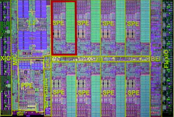
Each 'Synergistic Processing Elements' (SPE) is a
powerful processor in its own right, focused on one thing: churning through
single precision and double precision mathematical calculations. As each
SPE component is a subordinate part of the whole Cell processor, they can
dispense with a lot of the complex instruction queuing logic that a typical
modern single processor computer needs. Each SPE gets its orders from the
64-bit Power PC unit which handles the scheduling and parceling of data out to
the SPEs. Instead the focus is on speed.

Each SPE has 256KB of on-die memory allotted only to it, but instead of being
used as conventional cache memory, this small area of high-speed storage is
actually addressed almost like typical system RAM. The L1 cache memory
found in conventional processors is highly automated, making it simple to
program for but adding overhead. With the Cell processor, programmers can
dictate exactly how they wish their software to use the 256KB allotment
available to each SPE. This allows execution efficiency to be increased
with good software design. It also allows better memory management and
security from buffer overflows and other exploits.
Individual SPEs should be able to pass data to each other by storing it in
specific areas of the system memory, forming a chain of processing units each
performing a different operation on the data. Obviously this requires an
extremely fast interface between the system RAM and the SPEs, which the Cell has
in spades… More on this later.

