When
Intel released the i865PE/i875P alongside the Intel
Pentium 4C processors, the DDR memory game changed forever. With a DDR memory
controller now capable of running dual channel, the Pentium 4 was no longer to
be bandwidth limited as it had been with the i845 series. Those single channel
DDR chipsets, like the i845PE for instance, could only provide half the
bandwidth required by the Pentium 4 processor due to its single channel memory
controller.
As the new 800 MHz FSB Pentium 4 processors allowed users to hit never before
seen highs in terms of bus speed, many memory manufacturers were trying to
capitalize on the situation by releasing every increasing degrees of
"high speed" memory.
Unfortunately, to run the memory frequency at the same speed as the FSB (or a
1:1 ratio) almost all the high speed DIMM's (Dual Inline Memory Module) have to
have very lax timings. Think about it this way, a car built for drag racing can
go dead straight super fast, but cannot maneuver as well as an F1 race car.
Likewise, the F1 racer is good in the corners but will be left in the dust on
the drag strip. In other words, today's high speed memory modules are
built for one thing only, and that's top speed, where timings really aren't
considered all that much.
Confused about memory timings?
When one talks about memory timings they're basically talking about how long
the system has to wait for the memory to be in a ready state before data is
fetched or delivered.
 You could think about memory timings as
people working at a drive through restaurant; you place your order then wait for
the food to be ready. The lower the timings are, the faster the computer (and
quicker your order comes) is able to get data from the memory, and the faster
the rest of the PC will ultimately be.
This rule of thumb applies whether you're on an Intel or AMD based system. As
for why there aren't lower timings then 2-2-2-5, JEDEC (the memory governing
body) does not think it's possible for current dynamic memory
technology to run at 0 or 1.
When we refer to timings it is common to quote a four digit number separated
by dashes (ie. 2-2-2-5) The first number always represents CAS (Column Address
Strobe) Latency as it's usually the most important.
Next in line is RAS-to-CAS Delay (Row Address Strobe), RAS Precharge and
Act-to-Precharge Delay (which is always the final, and largest number).
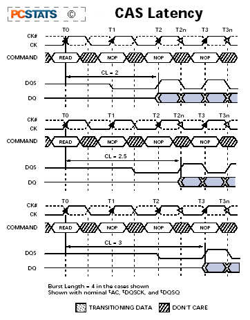
In the picture to the left here, we can see the the timing diagram from some
Crucial DDR333 memory. If we take this as an example for all subsequent memory
speeds, I think we should be able to illustrate just what all these 'timing'
numbers really represent.
The diagram shows timings of CAS2, CAS2.5 and CAS3 timings (marked as CL=2
for example). Note the vertical dashed lines which indicate a rise or fall of
the clock signal, since this is double data RAM, there are two such points per
'Time unit'.
CAS latency is the delay between the registration of a read command and the
availability of the first piece of output data. CAS latency is measured in clock
cycles. In the last of the three examples, a read command which is registered at
T0 (Time=0) is not valid until T3 (Time=3).
 With all things equal, a stick of DDR
memory capable of running 2-2-2-5 will make the computer operating experience
seem faster than a DIMM which may only run at 3-4-4-8. This is because the delay
from when the memory receives an instruction, retrieves the data,
and sends it back out is less.
Where it starts to get confusing is when you has the choice of
buying high speed memory with slow timings. Just about ever
PC3700+ rated memory module we've seen uses conservative timings after all. If
your answer would be to buy fast memory with tight timings,
I'm afraid you're going to be disappointed as there are no such modules
available yet. So, why are we still interested in fast memory with slow timings
then? Well, the answer goes something like this....

