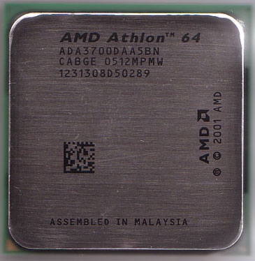
As someone
who has been in the overclocking biz since the days of the 486, I'm happy to see
how large this hobby has become. Now, on the heels of PCSTATS highly popular Athlon64 3500+ overclocking article comes
a new adventure with the Athlon64 3700+ processor! AMD's Athlon64 'Winchester' core has been around for a while now, but enthusiast overclockers who employ TEC or phase change cooling have been avoiding it in large part. The
reason being that the Winchester core apparently can become an unstable
overclocker if cooled too far below zero degrees Celsius. The problems vary
from system lock ups, to not POSTing at all.
With the
release of the AMD 'Venice' and 'San Diego' Revision E Athlon64
processors, the enthusiast crowd has been quietly hoping for a better turn of
luck. Both the Venice and San Diego Athlon64 cores are built with the same 90nm
manufacturing process as their predecessor, but incorporate an improved memory
controller and SSE3 instructions. The latter should not come as a surprise,
Intel has been licensing SSE technology to AMD for quite some time now. More
importantly for overclockers though, the Venice/San Diego cores are rumored to
have shaken off the cold bug that affected some Winchester core Athlon64
processors.
Cache size
is the only point differentiating the San Diego from Venice cores from each
other. Venice-based Athlon64 processors come with a traditional 512KB of L2
cache, while the San Diego core has 1MB of L2 cache. Interestingly, the Athlon64
3700+ processor is clocked at 2.2 GHz, the same speed as the Winchester-based
Athlon64 3500+ CPU. As we've seen in previous processor reviews, a larger L2
cache of the 3700+ can boost performance nicely...
 |
|
|
AMD Athlon64 3700+
Processor |
|
|
 |
| Tech Specs |
|
Clock:
2.2GHz
L1: 124KB
L2: 1024KB
Multipiler: 11x
Package: 939-pin
organic mPGA
Core:
90nm SOI
Vcore: 1.4V
Cost: $334USD
| |
|
Further Technical Details:
CPU-to-Memory Controller: 2.20GHz
Memory: Integrated 128-bit wide memory
controller
Types of Memory: PC1600, PC2100,
PC2700 and PC3200 DDR
HyperTransport Links:
1
HyperTransport Spec: 2GHz (2x 1000MHz /
DDR)
Effective data bandwidth: Up to 14.4
GB/sec (8GB/sec)
HyperTransport bandwidth
plus 6.4GB/sec memory bandwidth)
Fab
location: AMD's Fab 30 wafer in Dresden,
Germany | |
As you can see from the photo above, the AMD Athlon64
3700+ (retail) processor that fell prey to our overclocking bag of tricks is
based on the 'CABGE' stepping, and was built some time in March 2005. The retail
package includes a quiet aluminum heatsink/fan, some documentation and of course
the little AMD Athlon64 sticker. As this review is specifically focusing on the
overclockability of the Athlon64 3700+, we're going to skip our usual technology
discussions and go straight to the good stuff!
If you'd like to learn a bit more about what makes the
AMD Athlon64 processor tick, please read PCSTATS' extensive AMD Athlon64 4000+ processor review.
Russian Roulette with CPUs,
Memory and Videocards
First though, let's talk about some of the hardware that
was used in this overclocking adventure. Remember, PCSTATS staffers test
hardware all day long, so when it comes to choosing the best hardware for the
job we're pretty damn picky. That said, great hardware alone does not guarantee
super-fabulous speeds every time. One of the fundamental truths of overclocking
computer gear is that it's still very much the luck of the draw. From batch to
batch, and part to part, the varying tolerances and minor differences built
into components are what keep things exciting!
Okay, the motherboard used in this test setup is the very
popular overclocker-friendly DFI LANParty NF4 SLI-DR. Having a wide array of memory
to choose from by the likes of OCZ, Corsair, Geil, Kingston, PQI, Twinmos, etc.
we opted for a pair of Mushkin's new Redline XP4000 series.
I selected the DFI board for its awesome overclocking and
voltage adjustment options. The Hypertransport speed was kept at its default of
5X (tested up to 350 MHz) and the memory was running in sync with the
motherboard clock speed (unless otherwise stated) with timings of 2-2-2-5.
Memory voltage was set to a higher than normal 3.6V,
nForce4 chipset voltage was kept to 1.8V and LDT set to 1.5V throughout all
tests. These voltages were chosen because I didn't want the memory flaking out
before the motherboard or CPU might have. The above settings apply to both the
air-cooled and phase change-cooled overclocking tests. Got all that!?
If you're new to Overclocking and not sure what to do,
check out these two excellent Guides for some pointers: Overclocking the CPU and Memory and Overclocking the Videocard

